High-Performance Computer Architecture 26 | An Introduction to Memory, DRAM, SRAM
High-Performance Computer Architecture 26 | An Introduction to Memory, DRAM, SRAM
- An Introduction to Memory
(1) The Definition of Random Access Memory (RAM)
Random-access memory (RAM) simply refers to the fact that we can access any memory location by address without going through all the memory locations. The opposite definition is a sequential access tape, where we have to scan through the whole tape to get a memory location.
(2) Types of RAM
There are mainly two types of RAM,
- Statistic Random Access Memory (SRAM): the term “statistic” refers to the fact that SRAM retains its data while the power is supplied. So you are not going to lose any data if you are connected to the power. However, to implement an SRAM, we need to have several transistors per bit. This causes the SRAM to become expensive.
- Dynamic Random Access Memory (DRAM): “dynamic” means that we will lose data unless we refresh the data. Although we will lose data when we have DRAM, we only need to have 1 transistor per bit. Thus, we can get a lot more DRAM per unit area than SRAM.
(3) Inverters
Before we talk about the organizations of SRAM and DRAM, let’s first introduce the inverters. The inverters are also called the NOT gate which implements logical negation. It is denoted by,

Basically, there are 3 common ways to implement this NOT gate. We can use a PMOS (P-type Metal Oxide Semiconductor, P-type MOS), an NMOS (N-type MOS), or a CMOS (complementary MOS). The transistors we have introduced before are BJTs, which are less commonly used in electronic digital circuits. You can find an explanation about BJT vs. MOSFET from here.
- NMOS Inverter
We can easily create an inverter with an NMOS and a pull-up resistor. This design has a low manufacture cost but it will have disadvantages on the power consumption and processing speed.

- PMOS Inverter
Similar to the NMOS inverter, we can also create an inverter with a PMOS resister, which also has problems with power consumption and processing speed.

- CMOS Inverter
To deal with the problems on the power consumption and processing speed, we can use two MOSFETs instead of just one with a resister. This is called the CMOS inverter design.

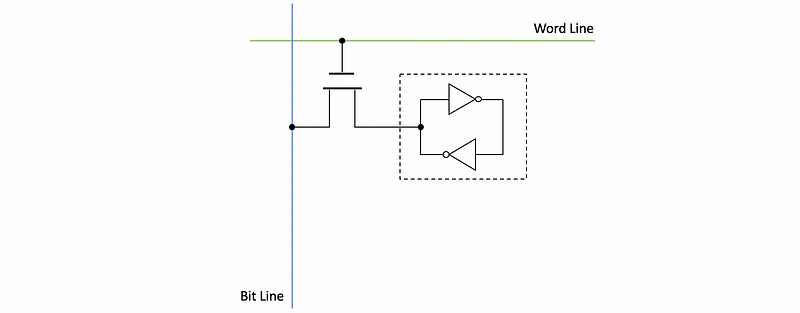
(4) The Organization of the SRAM
In the SRAM structure, remember what we have to do is that the SRAM should always keep the data in the memory cell until it is overwritten or the power is no longer supplied. This means that the memory cell should be able to keep the data.
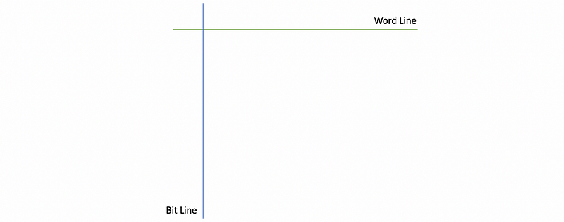
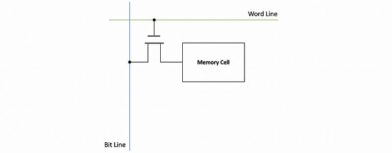
Also, each memory cell has a word line that acts to control the cell. The signal that accesses the cell to either read or write data is applied to the word line.
Perpendicular to the word lines is bit lines. The data that is being written into or read from the memory is found on the bit lines. So our memory is actually a matrix of cells.
A transistor should be used to connect the word line, the bit line, and the memory cell. If we want to access the memory cell, we should activate the word line, which opens the transistor and the transistor connects the bit line to the memory cell. Then if we want to write to the memory cell, we put the data we want to write at the bit line and the cell gets the value. If we want to read the data, we will get the value at the bit line to go away so that we can get a new value from the memory cell.
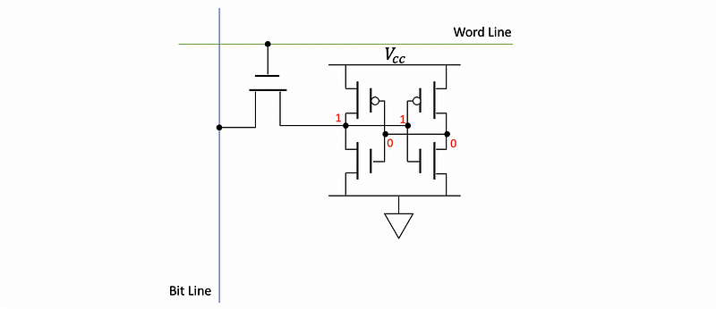
In SRAM, the actual memory cell consists of two CMOS inverters as we have talked about above.
Actually, each CMOS inverter has two CMOS transistors. The basic idea is that if you write a to the memory cell, the inverter on the right-hand side will flip it to 0. However, another inverter will then flip it to 1. So once the control transistor writes a value to the memory cell, the cell will keep its value until it is power-off.
But this can also lead to another problem. When we want to change the value of the cell, the existing value in the cell will against the new value we would like to write. For example, suppose the cell keeps the value 0 and we would like to write a 1, which means we must write an amplified 1 so that it can defeat the value of 0.
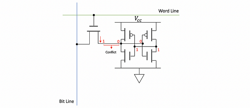
To make this defeating process easier, typically we have 2 of the control transistors and two bit lines for the same cell that have the opposite values (i.e. BL and BL-bar).
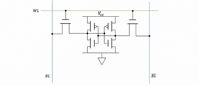
You can find out that for the SRAM, in order to maintain a bit of memory, we have to use 6 transistors, and this can be expensive.
(5) The Organization of the DRAM
Instead of using multiple transistors for storing the data as we have discussed for the SRAM, the main difference for the DRAM is that we only use 1 control transistor for 1 bit. The memory cell only consists of a capacitor that is used to keep the value of the data.
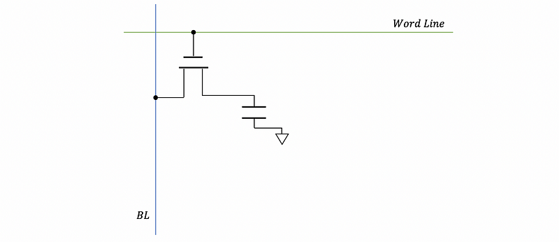
However, the main problem for this organization is that the control transistor is not a perfect switch so that there will be a little bit of leak from the transistor. Thus, the capacitor will slowly leak to the bit line and eventually, it gets empty, and we will lose this bit over time. To prevent this leakage, we have to periodically update the data in the capacitor.
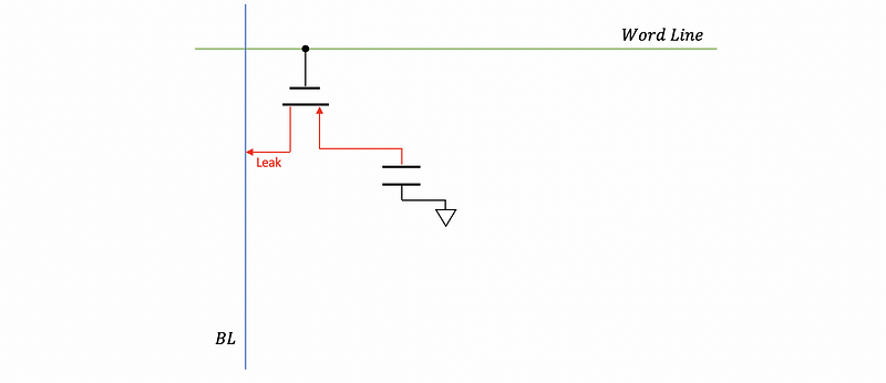
There is another problem called destructive read. This happens because when we read from the bit line, the capacitor drains into the bit line but it is no longer fully charged.
(6) Trench Cell
In the example above, we have built a DRAM memory cell by a transistor and a capacitor. However, this is not how we build a DRAM cell in reality. In fact, the transistor and the capacitor are built as a signal transistor in a technology called trench cell. By this means, we save the area of a capacitor.
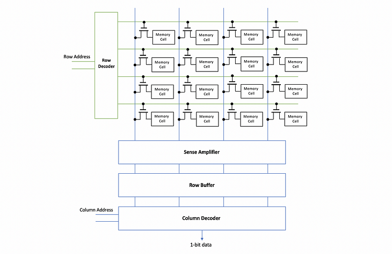
(7) The Organization of Memory Chip
In a real memory chip, we have
- Word lines that used to activate cells
- Row decoder decides which word line gets activated
- Row address to the row decoder that implies which word line to be activated
- Bit lines used to input the data to the memory cell
- Memory cells that are either relatively weak SRAM cells or DRAM cells with relatively small capacitors
- Sense amplifier connects all the bit lines. It senses the small changes on the bit lines and amplifies them
- Row buffer is a storage element that stores the correct values read from the whole row of cells after amplified by the sense amplifier
- Column decoder selects the correct bits smong the bit lines using the column address and then it outputs a single bit
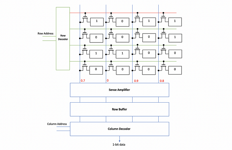
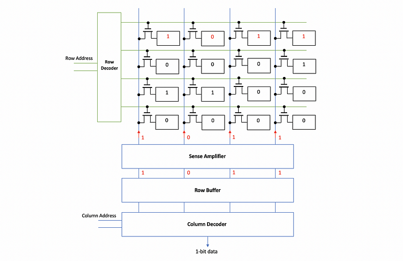
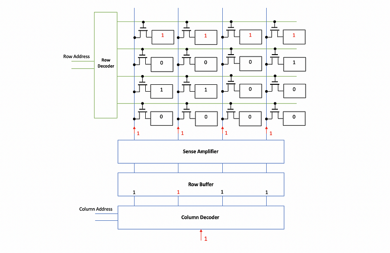
For example, the diagram of a 16-bit memory storage is as follows,
(8) The Organization of Memory Chip: An Example
Now, let’s see an example about the organization of the memory chip. Suppose we have a 16-bit memory storage chip with the data as follows,
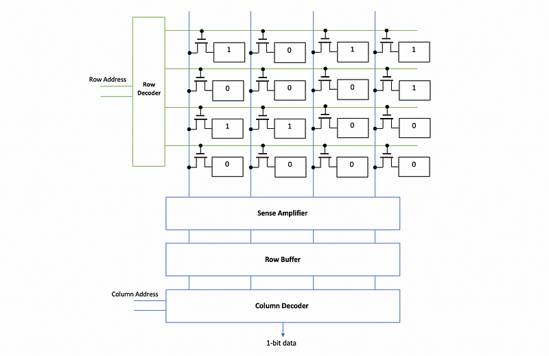
Suppose the row address is 00 and the column address is 01, let’s see the process of getting a 1-bit data from the memory. After decode the row address, we will choose the 0th row and then output the data of that row to the bit line. Note that the data we read may not be exactly the same as 1 before the amplifier.
After the amplifier, the correct value on each of the bit lines will be stored in the row buffer waiting for the column decoder.
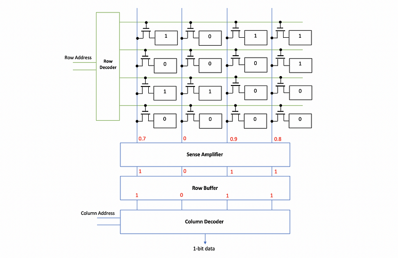
After decoding the column address, we can know that the data in the second bit line should be extract. Then we will get a value of 0.
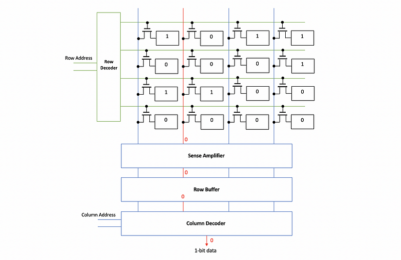
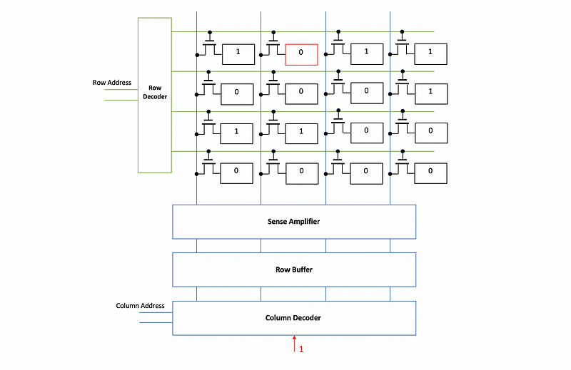
(9) The Organization of Memory Chip: A Problem
However, in the example above, there is a problem. When we get the data from the DRAM memory cell, the capacitor will no longer hold the data. This means,
In order to deal with this problem, after the sense amplifier amplifies the voltages, it will also drive the correct values back into the cells and so that the cells can get their values again.
We have talked about the destructive read of DRAM actually means that we have to have a read-then-write pattern. So we can not just wait long enough to get the value. What we should also do is to put the value back to the cell. This is a reason why DRAM is slower than SRAM.
Also, note that the cell doesn’t not strongly put the bit lines so that the sense amplifier needs more time to figure out what it has. After this read-then-write approach, the data in the capacitor have also been refreshed. The refresh process is really make sure that each of the rows is read every once in a while.
When we have a cache, the refreshes will become even more important. Because the most frequently accessed data will be stored in the cache and it will not be update automatically by the read-then-write approach. Suppose we have a DRAM memory cell that will automatically lose the data in time T, then in order to keep all the data in the memory, we have to read and write to every row (assume we have N rows) within this amount of time. We can not rely on the processor to read-then-write all the rows in time T, so we have to use a refresh row counter to trace which row should be refreshed.
(10) Write to DRAM Memory Chip
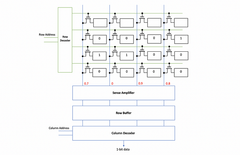
In the previous example, we have discussed how to read from the DRAM memory chip. The read-then-write approach is used to keep the data in the memory cell. But how to write to the memory? Let’s see an example. Suppose we want to write 1 to the second cell in the first row,
First of all, the data in the first row will be read to the row buffer as what we have done in the reading process.
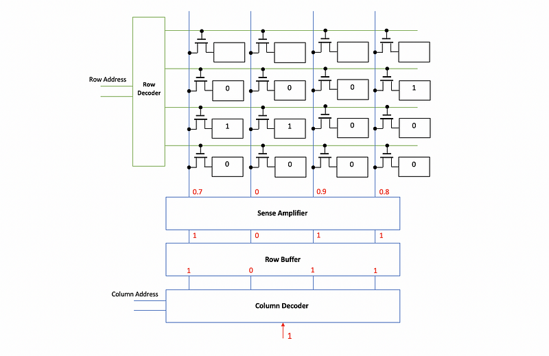
Then in the row buffer, the corresponding value we would like to write will be updated to the new value that we would like to assign.
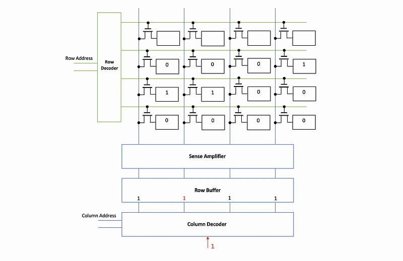
Then the data in the row buffer will be sent back to the cells because the first row is empty after we read from it.
You can find out that the writing process also follows the read-then-write approach.
(11) Fast-Page Mode
Once we have done a reading or writing process from the memory, the row buffer can retain the entire row. So then if we want to read from the same row, we don’t have to go through the row decoder, the sense amplifier, and row buffer mechanism again. What we can do is to directly read from the row buffer and just change the column address and get the data we want. This approaching of reading the data is called the fast-page mode. It is so-called with the term page because some people would like to call a row by page. And this page has nothing to do with the term page we have used for the virtual memory.
The fast-page mode has the following steps,
- Step 1. Opening a page: this is the first read from a row, which contains getting the row address, selecting the row, dispatching to the sense amplification, latching to the row buffer
- Step 2. Read/Write: if we then read or write to the same row, we can simply retrieve the data from the row buffer
- Step 3. Closing a page: if we finally decide to do something on another memory, we do something called closing the page. We will now write the values in the row buffer back to the row.
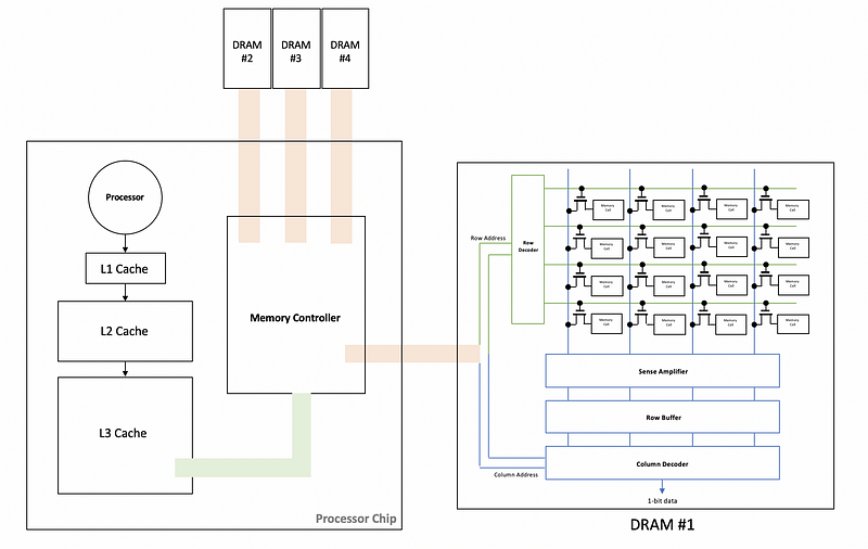
(11) Connecting DRAM to the Processor Chip
Suppose we have a three-level-cache processor, and if we have a cache miss in the L3 cache, we have to go to the memory to find the data. To find the data in the memory, and the L3 cache will send the address to the memory controller through the front-side bus. The memory controller is then used to analyze the address and send the address to the corresponding DRAM (because we can have multiple DRAMs connected to the processor) through the memory channel.
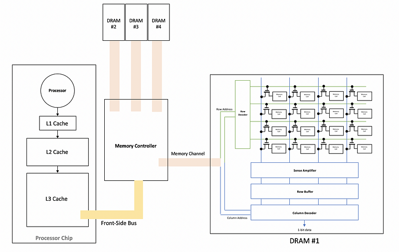
Thus, the L3 cache latency includes sending the request to the front-side bus, sending the page operations to the apporate DRAM channels, sending a request to read/write based on the column addresses, getting the data back to the memory channel, and finally the memory controller sends the data over the front side bus to the L3 cache.
This organization can be improved when we put the memory controller on the processor chip and then we can simply eliminate the front-side bus by using lots of on-chip wires, which saves the latency of L3 cache.